Sample Exam Questions
This exam paper provides a set of typical exam questions on the theme of computer architecture with sample solutions. If you have any comments or suggestions, or wish to contribute a question of your own, please get in touch with me.
Assembly Language
Problem 1
Convert the value in register r0 into its two’s complement form. However, you must not use either a subtraction operation or any other register.
Solution 1
The two’s complement of X is 2n – X. One way of forming the two’s complement is to invert the bits of X and add 1. The ARM lacks a NOT operation required to invert bits. However, we can use an exclusive OR with 1 to perform inversion because. Then we can add 1; that is,
EOR r0,r0,#0xFFFFFFFF ;invert r0
ADD r0,r0,#1 ;form two’s complement
Problem 2
Microprocessors have arithmetic and logical instructions such as ADD, SUB, AND and OR. However, multiplication instructions have characteristics that make them rather different from other arithmetic/logical operations. Give three reasons why the multiplication instruction differs from other arithmetic/logical operations.
Solution 2
Integer arithmetic and logical operations are applied to two m-
Integer addition and subtraction works with two’s complement arithmetic; for example
X – Y is performed by adding the two’s complement of Y to get X + (2n – Y) = 2n +
X – Y. This is the required answer apart from the leading 1 in the carry out position.
If we multiply these numbers we get X * (2n – Y) = 2nX – XY. The correct result in
2n-
Simple pencil-
Problem 3
What is the difference between little endian and big endian storage conventions?
Solution 3
The term endian is used to describe how bytes are ordered in computer memory. In
the days of the 8-
The ability to address individual bytes leaves one problem. If we call the four bytes
of a 32-
To complete
Problem 4
A particular 32-
Solution 4
The computer instruction is composed of op-
The 95 op-
Microprogramming and Architecture
Problem 1
The following figure gives the structure of a simple digital computer with a single
bus. Since there is only one bus, it is necessary to have at least one register in
an ALU input path. A register is also provided in the ALU output path. Note that
there are four memory data registers. One holds data to be written into memory. Three
registers hold data read from memory. The IR holds the instruction read during a
fetch phase, the MDR holds the data read from memory, and the literal register holds
and literal that form part of an op-
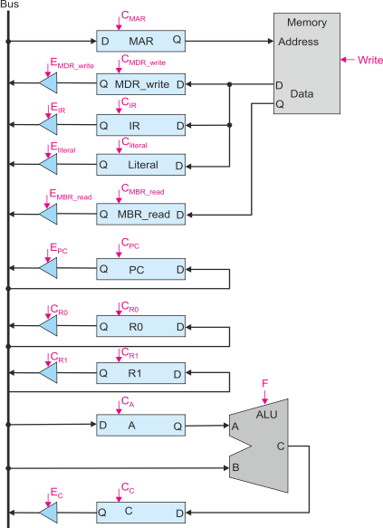
The control signals are the tristate driver enables, the register clocks, the memory write control, and the ALU function control.
- Write the microcode to perform a fetch cycle. You may assume appropriate ALU function codes are available.
- Write the microcode to perform ADD r0,r1,r0.
- Write the microcode to perform STR r0,1234 which is refined as [1234] ¬ [r0]
- Write the microcode to perform LDR r0,[r1] which is defined as [r0] ¬ [[r1]]
Solution 1
a.
During a fetch cycle the contents of the program counter are used to access the next instruction in memory. That is read and then loaded into the instruction register. The program counter is then incremented to point to the next instruction.
The steps are:
[PC] ¬ [MAR]
[IR], [literal] ¬ [[MAR]] Note that the instruction is read into the literal register as well as the IR
[PC] ¬ [PC] + 1 Note that the PC is incremented by 1 (if this were a 32 bit byte addressed machine the increment would be 4).
Translating into actual routing we get:
EPC, CMAR Copy PC to MAR
CIR,Cliteral Read memory and copy to IR and literal register
EPC, F=Increment, Cc Copy PC to B input of ALU, select increment function, copy result to C register
Ec, CPC
Performance
Problem 1
Consider a processor with the characteristics below. We give the number of cycles per operation for each of its instruction classes, and the actual number of operations performed by the members of each instruction class when the same problem is compiled using two different compilers.
Instruction class Cycles per instruction Instructions for compiler A Instructions for compiler B
Arithmetic and logical 1 240 280
Multiplication 3 20 0
Load from memory 6 200 200
Branch taken 3 80 80
Branch not taken 1 80 6
- What is the average number of clocks per instruction required by compiler A and compiler B?
- What is the execution time for the programs using compiler A and compiler B assuming a clock of 1 GHz?
- Which is the faster compiler and by how much?
Solution 1
- a. To obtain the total time we multiply the number of instructions executed by the number of cycles required by that instruction. and sum the result across all instruction groups. For compiler A we get:
240 x 1 + 20 x 3 + 200 x 6 + 80 x 3 + 80 x 1 = 240 + 60 + 1200 + 240 + 80 = 1,820 cycles.
The average number of cycles per instruction = total cycles/total instructions
= 1,820/(240+20+200+80+80) = 1,820/620 = 2.94 cycles/instruction.
For compiler B we get:
280 x 1 + 0 x 3 + 200 x 6 + 80 x 3 + 6 x 1 = 280 + 0 + 1200 + 240 + 6 = 1,726 cycles.
The average number of cycles per instruction is 1,726/(280+0+200+80+6) = 1,726/566 = 3.05 cycles/instruction.
- At 1 GHz, the clock period is 1 ns. The time to execute the code in nanoseconds is the clock time multiplied by the number of instruction. For compiler A this is 1 ns x 1,820 = 1,820 ns. For compiler B the corresponding time is 1 ns x 1,726 = 1,726 ns.
- To compare the performance of system P relative to system Q, we divide the time taken by Q by the time taken by P. In this case, compiler B is faster than compiler A and the relative performance improvement is 1,820ns/1,1726ns = 1.054.
Cache Memory
Problem 1
Consider a computer operating at 0.5 GHz (basic instruction cycle time) with a single
level, writeback, data cache memory. The processor-
- What is the cost of a miss in terms of clock cycles?
- What is the average data access time in clock cycles?
Solution
a.
We have to put together several factors to answer this problem. On a hit to cache, the access time is 1 clock cycle (because we said the cache operated at the same speed as the CPU).
On a cache miss, memory must be accessed. This requires a latency of 70 ns before
data can be delivered. After that, we can access a 64-
However, on a write access it will be necessary to first write back the cache line to memory. This requires 160 ns. Since only 30% of memory accesses are writes, the average penalty due to writeback operations is 0.3 x 160 ns = 48 ns.
The average time following a miss is 230 ns + 48 ns = 278 ns. Since a clock rate of 0.5 GHz corresponds to a clock period of 2 ns, the miss penalty is 230/2 = 115 cycles.
b.
If the miss rate is 4% or 0.04, the average cycle time is cache access time x hit rate + memory access time x miss rate= 1 x (1 – 0.04) + 115 x 0.04 = 0.96 + 4.60 = 5.56 cycles.
Superscalar Processing
Problem 1
Consider the following code:
ADD r0,r1,r2
ADD r3,r0,r4
MLT r3,r3,r5
STR r4,[r8]
LDR r11,[r9]
ADD r7,r11,r7
SUB r12,r6,#4
MLT r10,r1,r6
ADD r3,r3,#1
- Assuming a non-
superscalar processor with the code order unarranged (i.e., in the above sequence) where an integer instruction takes 1 cycle, a load 2 cycles, a store 1 cycle, and a multiply 2 cycles, how long does it take to execute the code. Assume that a RAW data dependency introduces 1 stall cycle.
- The same code is executed on an in-
order superscalar processor that permits two instructions to be executed simultaneously. The same timing constraints apply as in part a. How many cycles are required?
- The same code is executed on an out-
of- order (OOO) superscalar processor that has the same timing characteristics as part b. How many cycles are required?
Solution 1
a.
The following code repeats the sequence in the question adding stall cycles as necessary
for read-
Cycle 1 ADD r0,r1,r2
Cycle 2 Stall due to RAW on r0
Cycle 3 ADD r3,r0,r4
Cycle 4 Stall due to RAW on r3
Cycle 5 MLT r3,r3,r5
Cycle 6 Stall due to multiply
Cycle 7 STR r4,[r8]
Cycle 8 LDR r11,[r9]
Cycle 9 Stall for load
Cycle 10 ADD r7,r11,r7
Cycle 11 SUB r12,r6,#4
Cycle 12 MLT r10,r1,r6
Cycle 13 Stall for multiply
Cycle 14 ADD r3,r3,#1
b.
In this case, we can perform two operations at the same time as long as one instruction
doesn’t use the result generated by another. Because the first three instructions
have RAW dependencies, they must be executed sequentially with the appropriate delays
added. Moreover, because out-
Cycle Pipe 1 Pipe 2
1 ADD r0,r1,r2 Stall (no instruction)
2 Stall Stall (no instruction)
3 ADD r3,r0,r4 Stall (no instruction)
4 Stall Stall (no instruction)
5 MLT r3,r3,r5 STR r4,[r8]
6 Stall LDR r11,[r9]
7 Stall (no instruction) Stall
8 SUB r12,r6,#4 ADD r7,r11,r7
9 MLT r10,r1,r6 ADD r3,r3,#1
10 Stall
c.
In this case we can execute code out of order as long as there is no data dependency. Now we have managed to keep both pipes reasonably happy and there are no completely lost cycles. The execution time is now 7 cycles which halves the original scalar value.
Cycle Pipe 1 Pipe 2
1 ADD r0,r1,r2 STR r4,[r8]
2 Stall LDR r11,[r9]
3 ADD r3,r0,r4 Stall
4 Stall ADD r7,r11,r7
5 MLT r3,r3,r5 SUB r12,r6,#4
6 Stall MLT r10,r1,r6
7 ADD r3,r3,#1 Stall
Cache Memory
Problem 1
A computer system has a 64 KB level 1 cache and a 1 MB level 2 cache. The L1 has an access time of 2 cycles. The L2 cache has an access time of 10 cycles and the main store an access time of 300 cycles. Accesses to L1, L2 and main store take place in parallel. The L1 cache has a miss rate of 4% and the L2 has a miss rate of 25%. What is the average access time of the memory system?
Solution 1
The average access time is the access time to L1 cache plus the access time to L2 cache plus the access time to main store divided by the total number of accesses.
The access time to L1 cache is the hit rate multiplied by the cache access time = (1 – 0.04) x 2 cycles = 0.96 x 2 = 1.92 cycles.
The access time to L2 cache is the fraction of time for which L1 misses multiplied by the L2 hit rate multiplied by the L2 access time. This is: 0.04 x (1 – 0.25) x 10 cycles = 0.04 x 0.75 x 10 = 0.3 cycles.
The main store has to deal with misses from both L1 and L2 caches. The average time is L1 miss rate x L2 miss rate x 300 cycles. This is: 0.04 x 0.25 x 300 = 3 cycles.
The average access time is 1.92 + 0.30 + 3.00 = 5.22 cycles.
Problem 2
Suppose that the system in problem 1 is to be modified to improve the average access time by 10%. The modification involves changing the size of the L2 cache to increase its hit rate. What hit rate would the L2 cache have to achieve to provide the 10% improvement?
Solution 2
The new access time must be 90% of the original access time; that is 0.9 x 5.22 = 4.698 cycles.
Using the same equation as in Problem 1 we have:
Average time = 0.96 x 2 + 0.04 x (1 -
Consequently, 1.96 + 11.6 x L2miss = 4.698 and L2miss = (4.698 – 1.960)/11.6 = 0.236 (23.6%).
Secondary Memory
Problem 1
Describe the fundamental differences between hard drives (HDDs) and SSDs, and explain their relative advantages and disadvantages?
Solution 1
A hard disk is an electromechanical device that stores data along concentric tracks on the surface of a rotating platter. The platter is coated with a ferromagnetic material that can be magnetized to store data. HDDs are mechanical miracles because the magnetic particles are tiny and a read/write head has to be positioned accurately over a specific track as the disk rotates. Unfortunately, it is not possible to increase the speed (access time) of HDDs. Although HDD storage capacity has increased by six orders of magnitude since their introduction, their access time has hardly changed. Because of their mechanical nature HDDs are sensitive to vibration and shock and sudden failure.
The HDD is a serial access device and its access time is made up of rotational latency (the time for the disk to rotate until the data is under the read/write head) plus seek time (the time for the read/write head to step to the desired track) plus the physical read/write time one the desired track,sector has been located. The access time is random and can be long. Moreover, if a file is fragmented across the surface of the disk, an access may require multiple seeks and rotational latencies.
An SSD, solid state disk, is simply a large flash memory array that appears to the computer as a hard disk. Consequently, an SSD is physically robust. It is not prone to shock or vibration. More importantly, it is a random access device and the time to read/write data is not dependent on the location of the data. Consequently, file fragmentation is not an issue.
SSDs use less power than HDDs which is of importance in mobile systems (and saves energy costs).
SSDs have one significant limitation. Because writing to flash memory physically damages the memory cell, each cell has an average life after which it fails. Techniques have been devised (called wear levelling) to distribute writes evenly throughout the memory by moving blocks of data around to maximize the life of an SSD.
At the moment SSDs are far more expensive than HDDs costing approximately ten times per stored bit. It is expected that the cost of SSDs will continue to decline.